Exploring the impact of Altium Auto Route on modern PCB design opens up a world of possibilities. Let's delve into how this innovative tool revolutionizes the way PCB layouts are optimized, offering a glimpse into the future of electronic design.
Altium Auto Route streamlines the routing process, simplifying complex tasks and enhancing design efficiency. This article will guide you through the key features, challenges, and tips for maximizing the potential of Altium Auto Route in PCB design.
Introduction to Altium Auto Route in PCB Design
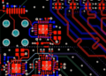
Altium Auto Route is a feature in Altium Designer software that automates the process of routing connections between components on a printed circuit board (PCB). This tool plays a significant role in modern PCB design by simplifying the routing process and optimizing the layout for improved performance.
Simplification of PCB Routing with Altium Auto Route
- Automatically generates connection paths between components, reducing manual effort and potential errors.
- Ensures efficient use of space on the PCB by finding the shortest and most optimal routes for signal traces.
- Allows designers to focus on critical design aspects by handling repetitive routing tasks swiftly and accurately.
Benefits of Using Altium Auto Route for PCB Layout Optimization
- Improves design productivity by saving time on routing tasks and enabling faster iterations of PCB layouts.
- Enhances signal integrity by minimizing signal interference and crosstalk through intelligent routing algorithms.
- Facilitates design collaboration by providing clear and organized routing paths that are easy to understand for team members.
Key Features of Altium Auto Route

Altium Auto Route offers a range of features that streamline the PCB design process, providing efficiency and accuracy compared to traditional manual routing methods.
1. Intelligent Routing Algorithms
Altium Auto Route utilizes intelligent routing algorithms to automatically route connections based on design rules and constraints. This feature helps in optimizing the layout and reducing the chances of errors in routing.
2. Real-time Design Feedback
One of the key features of Altium Auto Route is the real-time design feedback it provides. Designers can instantly see how changes impact the routing and make adjustments accordingly, leading to quicker iterations and improved design quality.
3. Interactive Routing Tools
Altium Auto Route offers interactive routing tools that allow designers to manually adjust routes while still benefiting from the automation features. This enables greater control over the routing process and ensures the design meets specific requirements.
4. Differential Pair Routing
Another important feature of Altium Auto Route is the ability to handle complex routing scenarios such as differential pairs. The software can automatically route these pairs while maintaining the required spacing and length matching, saving time and reducing the likelihood of errors.
5. Design Rule Checking
Altium Auto Route includes robust design rule checking capabilities that help detect and resolve potential issues early in the design process. This feature ensures that the final PCB layout complies with industry standards and design guidelines.
6. Seamless Integration
Altium Auto Route seamlessly integrates with other tools in the Altium Designer software suite, providing a cohesive design environment. This integration enhances workflow efficiency and collaboration among team members working on the same project.
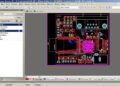
Understanding the Auto-routing Process in Altium Designer
When it comes to PCB design, using the auto-routing feature in Altium Designer can greatly streamline the process and save valuable time. Understanding how to effectively utilize this tool is crucial for achieving optimal results in your designs.
Step-by-Step Process of Using Altium Auto Route in PCB Design
- Start by selecting the components you want to connect on your PCB layout.
- Access the auto-routing feature in Altium Designer and define the nets that need to be routed.
- Set up the design rules and constraints to guide the auto-routing process.
- Initiate the auto-routing tool and let Altium Designer automatically create the connections between the selected components.
- Review the auto-routed traces and make any necessary adjustments to ensure the design meets your specifications.
Parameters and Settings Customizable in the Auto-routing Process
- Trace width and spacing: Adjusting these parameters can help optimize signal integrity and prevent interference between traces.
- Routing topologies: You can choose different routing strategies such as orthogonal, hug-and-push, or obstacle-avoidance to suit your design requirements.
- Layer assignment: Control the layers on which traces are routed to efficiently utilize the PCB real estate.
- Net classes: Define specific routing rules for different net classes to ensure consistency across the design.
Tips for Optimizing the Auto-routing Results in Altium Designer
- Use design rules to enforce constraints and ensure the auto-router follows specific guidelines.
- Segment your design into manageable sections to improve routing efficiency and reduce complexity.
- Manually route critical or high-speed signals to maintain signal integrity and minimize interference.
- Regularly review and iterate on the auto-routed traces to fine-tune the design and address any routing issues.
Challenges and Limitations of Altium Auto Route
When working with Altium Auto Route for PCB layout, there are certain challenges and limitations that designers may encounter. Understanding these can help in finding solutions and workarounds to optimize the auto-routing process.
Common Challenges Faced with Altium Auto Route
- Difficulty in routing high-speed signals: Altium Auto Route may struggle to efficiently route high-speed signals, resulting in signal integrity issues.
- Complex component placement: Auto-routing may face challenges when dealing with complex component placements, leading to routing errors.
- Routing congestion: Auto-routing algorithms may not always effectively manage routing congestion, especially in densely populated PCB designs.
Limitations of Auto-Routing in Complex PCB Designs
- Lack of intelligent decision-making: Altium Auto Route may not always make the most optimal routing decisions, leading to suboptimal results.
- Inability to handle specific design constraints: Auto-routing may struggle with meeting certain design constraints, such as impedance control requirements.
- Difficulty in routing differential pairs: Routing differential pairs accurately and efficiently can be a limitation of auto-routing in complex PCB designs.
Solutions and Workarounds for Overcoming Challenges with Altium Auto Route
- Manual intervention: Designers can manually adjust the routes generated by Altium Auto Route to overcome routing challenges and ensure signal integrity.
- Pre-routing strategies: Pre-planning routing strategies and component placements can help mitigate routing congestion and complex routing issues before using auto-routing.
- Using design rules: Setting up specific design rules and constraints can guide the auto-routing process to meet the required criteria and improve routing outcomes.
Ending Remarks
In conclusion, Altium Auto Route stands as a game-changer in modern PCB design, paving the way for faster, more accurate, and optimized layouts. Embrace the power of automation and unlock new possibilities in your PCB projects with Altium Auto Route.
Essential FAQs
How does Altium Auto Route simplify the PCB routing process?
Altium Auto Route automates the routing of traces, making it faster and more efficient compared to manual routing methods.
What are the main features of Altium Auto Route?
Some key features of Altium Auto Route include automated trace routing, optimization algorithms, and customizable routing parameters.
Are there any limitations to using Altium Auto Route?
Altium Auto Route may face challenges in complex PCB designs where manual intervention is required for specific routing requirements.


